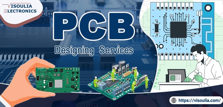
In the rapidly advancing world of technology, mastering PCB designing services is essential for anyone looking to create electronic products that stand out. Whether you're an engineer, a hobbyist, or a startup founder, understanding the intricacies of PCB design can elevate your projects and ensure their success. At Visoulia Electronics, we specialize in providing top-notch PCB designing services, and today, we’ll guide you through six simple steps to master these essential skills.
1: Understand the Basics of PCB Design
Before diving into complex designs, it’s crucial to understand the fundamentals of PCB design. A printed circuit board serves as the foundation for electronic components, facilitating their interconnections. Key concepts to grasp include:
-
Components: Familiarize yourself with various electronic components like resistors, capacitors, and integrated circuits (ICs).
-
Schematic Diagrams: Learn how to create and read schematic diagrams, which visually represent the electrical connections between components.
-
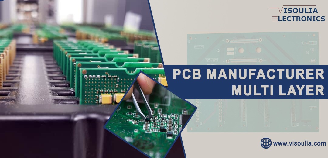
Layering: Understand the difference between single-layer and multi-layer PCBs, as well as how to choose the right option for your project.
At Visoulia Electronics, we recommend starting with online courses or tutorials that cover these basics to build a solid foundation.
2: Choose the Right PCB Design Software
Having the right tools is critical for successful PCB design. There are numerous software options available, each with its unique features and capabilities. Some popular choices include:
-
Altium Designer: Known for its powerful features and user-friendly interface, ideal for professional-level designs.
-
Eagle: A popular choice for hobbyists and small businesses, offering a free version with limited capabilities.
-
KiCAD: An open-source software that provides a comprehensive set of tools for PCB design.
At Visoulia Electronics, we utilize advanced software to create precise and efficient designs, but your choice will depend on your specific needs and budget. Experiment with a few options to find the one that suits you best.
3: Develop a Schematic
Once you’re familiar with PCB design fundamentals and have selected your software, it’s time to create your schematic. This step is vital as it forms the blueprint for your PCB layout. Here’s how to approach it:
-
Component Placement: Start by placing all necessary components in the schematic.
-
Wiring Connections: Use the software tools to connect components based on their intended electrical pathways.
-
Verification: After completing your schematic, run verification checks to ensure there are no errors in connections.
A well-structured schematic is crucial for an effective PCB layout. At Visoulia Electronics, we emphasize the importance of this step to ensure a smooth design process.
4: Design the PCB Layout
With a verified schematic in hand, the next step is to translate it into a PCB layout. This is where your design will take physical form. Follow these guidelines for effective layout design:
-
Component Placement: Arrange components logically, minimizing the distance between connected parts to reduce signal loss and interference.
-
Trace Routing: Carefully route traces to connect components, ensuring they are wide enough to handle the required current without overheating.
-
Ground and Power Planes: Incorporate ground and power planes to reduce noise and improve overall performance.
This stage can be complex, but remember that practice makes perfect. Don’t hesitate to refer to examples or consult with experts at Visoulia Electronics if needed.
5: Prototyping and Testing
Once your PCB layout is complete, the next step is to create a prototype. This involves fabricating a small batch of PCBs to test the design under real-world conditions. Here’s how to approach this phase:
-
Fabrication: Send your design files to a manufacturer for fabrication. Make sure to choose a reputable provider that meets your quality standards.
-
Assembly: Once fabricated, assemble the components on the PCB. This can be done manually or through automated assembly services.
-
Testing: Conduct thorough testing to ensure the PCB functions as intended. Check for issues like signal integrity, power distribution, and component functionality.
At Visoulia Electronics, we emphasize rigorous testing to catch any issues early in the process, allowing for timely adjustments.
6: Iteration and Improvement
The final step in mastering PCB designing services is to iterate based on your testing results. PCB design is rarely perfect on the first try, and improvements are often necessary. Here’s how to approach iteration:
-
Analyze Test Results: Look for any performance issues, such as overheating or signal loss, and identify their root causes.
-
Make Adjustments: Modify the PCB design based on your findings. This might involve changing trace widths, repositioning components, or even revisiting your schematic.
-
Retest: After making changes, create another prototype and repeat the testing process to ensure all issues have been resolved.
At Visoulia Electronics, we view iteration as a vital part of the design process, ensuring that the final product meets all quality and performance standards.
Conclusion
Mastering PCB designing services is a valuable skill that can greatly enhance your capabilities in the electronics field. By following these six simple steps—understanding the basics, choosing the right software, developing a schematic, designing the layout, prototyping, and iterating—you’ll be well on your way to creating effective and reliable PCBs.
At Visoulia Electronics, we are committed to helping you navigate this journey. Whether you’re looking for professional PCB designing services or guidance on your projects, our team of experts is here to support you every step of the way. Embrace the world of PCB design, and unlock new possibilities for your electronic innovations!